New Technique Reveals 3-D Shape of Nanostructure's Polariton Interaction

Xu's new technique could help researchers characterize how the electrical field is distributed around a nanostructure like graphene, the lattice-like structure of which is depicted in the illustration above. (Image credit: iStock-Rost-9D)
Nanostructures are the holy grail of new materials.
The wonder material graphene, for example, is a single layer of carbon atoms arranged in a hexagonal pattern that, because of its conductivity, flexibility, transparency and strength, has the potential to create more efficient solar cells, smaller and faster electric circuits and microchips, transparent displays, and high density capacitors and batteries.
According to Xiaoji Xu, assistant professor of chemistry, another quality that makes nanomaterials like graphene so special is their ability to generate a physics phenomenon called a polariton.
Polaritons are quasiparticles resulting from a strong coupling of electromagnetic waves with an electric or magnetic dipole-carrying excitation—referred to by some as a light-matter coupling. Polaritons make it possible for nanostructures to confine—and compress—light around the material.
The ability to compress light is key to scaling down devices for future optical communications and computing. It could also lead to sensing at a scale below one nanometer, which is important for achieving biomedical advances in disease detection, prevention and treatment.
The challenge for people studying these materials, says Xu, is how to reveal—and characterize—the polaritons at the nanoscale because no conventional microscope can do that.
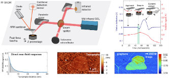
Now Xu and his team have found a way to reveal the 3-D shape of the polariton interaction around a nanostructure. Their technique improves upon the common spectroscopic imaging technique known as scattering-type scanning near-field optical microscopy (s-SNOM). The team’s method, called peak force scattering-type scanning near-field optical microscopy (PF-SNOM), works through a combination of peak force tapping mode and time-gated light detection. The researchers have detailed their work in an article called: “Tomographic and multimodal scattering-type scanning near-field optical microscopy with peak force tapping mode” (DOI: 10.1038/s41467-018-04403-5) published online on May 21, 2018 in Nature Communications. In addition to Xu, the paper’s co-authors include Haomin Wang, Le Wang and Devon S. Jakob, Ph.D. students in Xu’s lab.
In the paper, the authors state: “PF-SNOM enables direct sectioning of vertical near-field signals from a sample surface for both three-dimensional near-field imaging and spectroscopic analysis. Tip-induced relaxation of surface phonon polaritons are revealed and modeled by considering tip damping.”
According to the researchers, PF-SNOM also offers an improved spatial resolution of five nanometers, rather than the typical ten nanometers offered by the traditional s-SNOM.
“Our technique could be beneficial to scientists studying nanostructures, enabling them to better understand how the electrical field is distributed around a given nanostructure,” says Xu.
Their PF-SNOM characterization method is not only more direct than existing techniques, it can also simultaneously obtain the polaritonic, mechanical and electrical information.
With one measurement, explains Xu, multiple modes of information can be obtained—a unique advantage.
The development of PF-SNOM grew out of the team’s study of gap mode: When two plasmonic structures approach within a few nanometers, there is a huge enhancement of the plasmon intensity in the gap between the two structures as energy is transferred from one structure to the other. With their ability to narrow this gap mode response in simulations, the researchers decided to try to extend it to non-gap mode—when increasing the distance between the atomic force microscopy (AFM) probe tip and the sample.
“Using an AFM tip, we measured the scattered light as a function of tip-sample distance,” explains Wang, a Ph.D. student in Xu’s lab and a co-author on the paper. “We then gathered information at different tip-sample distances and combined all this layered information together to obtain the tomographic image and reveal the 3-D polariton structure.”
Interestingly, when the team began their experiments they expected a different outcome. However, during the simulations, they observed a special shape of light scattering and saw there was an obvious gap mode enhancement.
“It turned out that we could section the light in different tip-samples distances and use those signals to view the near-field response at different layers and in vertical directions,” says Wang.
He adds: “Though this work was done with infrared, in principle it could also be extended to other frequencies, such as visible and terahertz.”
Posted on:


